


New efficiencies for SHJ solar cells thanks to collaboration between longi, Sun Yat-Sen University and TU Delft
Another step forward for solar cells in silicon heterojunction (SHJ). Thanks to the in-depth study of the flow of charge carriers within the cellular architecture, a group of experts found a way to increase the efficiency of these devices with small but decisive changes. Interventions that could be quickly imported by the solar industry by expanding the scope of the photovoltaic SHJ.
But to understand the type of innovation being developed, we need to take a few steps back. Heterojunction silicon solar cells represent a hybrid phoyovoltaic technology, which combines aspects of conventional crystalline silicon units with thin film. The cellular architecture employs selective contacts for electrons and their amorphous silicon gaps appropriately doped. And it is precisely these layers and their doping that depend on the electrical performance of this technology.
From laboratory to factory
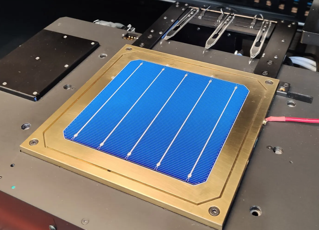
The international team, composed of experts from the LONGi Green Energy Technology, researchers from Sun Yat-Sen University and the Delft University of Technology, has optimized the design of the SHJ solar cell using a contact layer of nanocrystalline silicon gaps. It is a level long known as theoretical possibility, but never put into practice successfully.
The new contact – the result of a long work of modeling and study of flows – is able to transfer electricity with a much lower resistance; This results in a higher conversion efficiency than any other type of solar cell made of crystalline silicon. The technicians of the LONGi have brought this innovation on a standard industrial level silicon wafer, making it almost immediately applicable in the production of photovoltaic panels.
Read also Perovskite-silicon solar cells: 28.2% efficiency
In detail, work on the new SHJ solar cells reached certified conversion efficiencies of up to 26.81% and filling factors of up to 86.59% on industrial grade silicon wafers (274 cm2, size M6). “It’s great to see in real and large devices what we theoretically expected to be the best combination for the contact layers of gaps,” says Paul Procel, researcher at TU Delft. The results of the research were published on 4 May in Nature Energy.